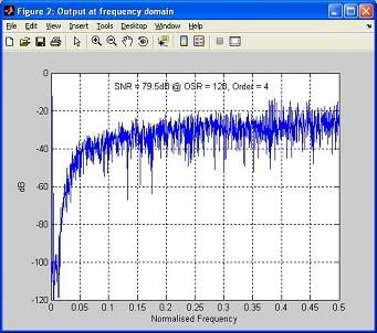
 This is the output for my fyp, sigma delta modulator. Generally, the noise shaping is working; notice how the low frequency components have lower noise compared to the higher frequency ones. This is because the low frequency noise has been "shifted" to the higher frequency part so that the signal of interest, which is in the lower frequency domain, is not affected by noise.
However, the result is far from expectation. 80dB of SNR is a far cry from the desired 120+dB that is required of a 20-bits sigma delta modulator. Sad. Sibeh sian. =((
And most people reading this dunno what i talking about. Also sibeh sian. No one can help me..
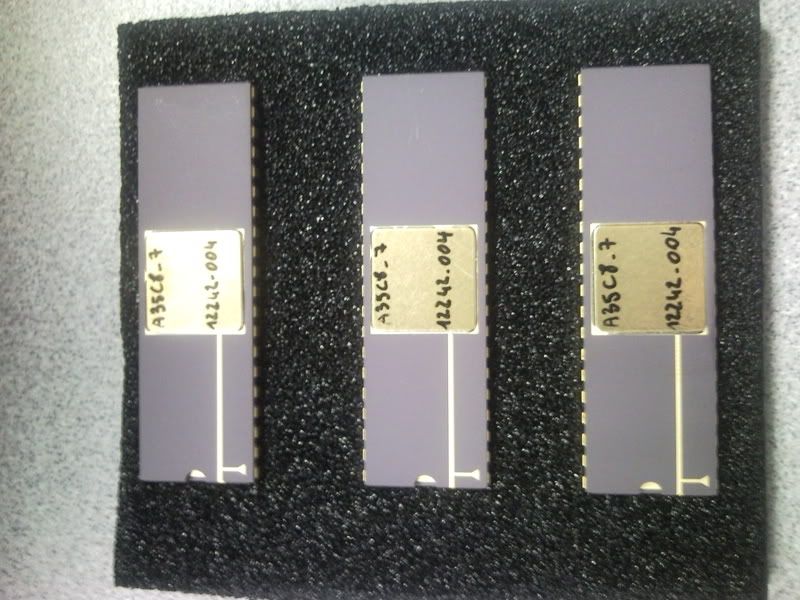
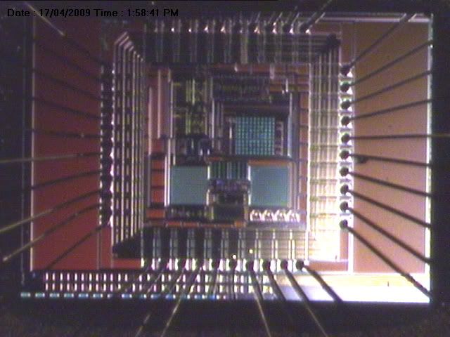
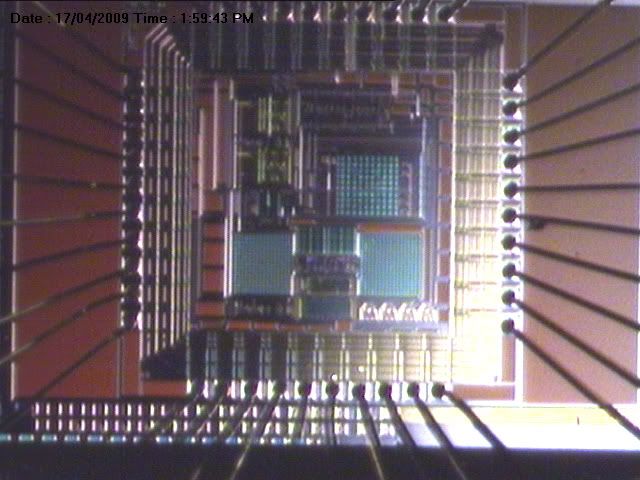
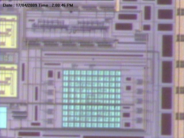
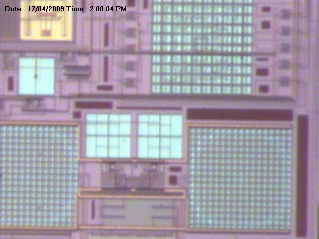
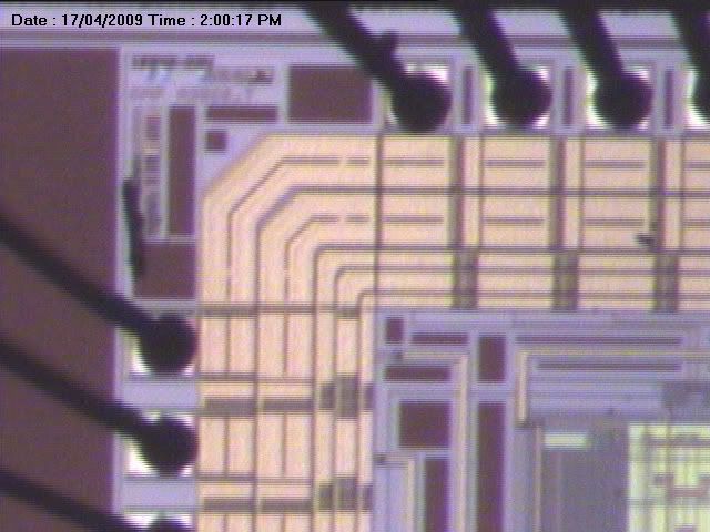
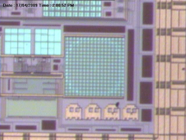
Yay, we just got back our chip, the one we spent one sem to design. So before sending for fabrication, our design was working pretty fine. Now that the real thing is fabricated, will it still work as we intended? That will be the task for us this semester, to perform all kinds of test on the chip to verify our design.

Initial test shows some system working fine. The ADC seems to be ok, but only 1 input tested. LNA seems to have lots of problems. Bandgap is ok. More tests will be perform for the next few weeks and if it works, yay! If not... then pray for at least a b+... lol
 Last friday was the official tape out date for EE4410. (Tape out in electronics terms is to submit the circuit design for fabrication.) So now that means we have nothing to do for this module till the next semester when the chip comes back, or at least close to nothing cos the foundry shoots back to us with some DRC(Design rules check) errors once in a while and we have to try to resolve those.
Sucks, now i having problem with my FYP, dunno why the results weird weird one.
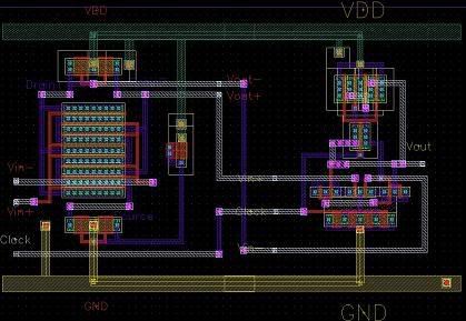 Yay, completed the layout design of my comparator and it passed the DRC and LVS test as well as the post-layout simulation. Most of the rest of the parts are completed too, now what's left is to stitch up the different parts and do the final overall system simulation. And if it meets our specs, that basically concludes the module! Woot! (at least for this semester that is)
Then i can start doing my FYP, too long never touch liao.. haha.
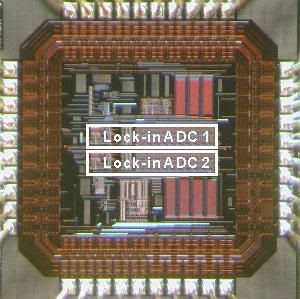
EE4410 (Integtated circuit and system design), it cost around $6k to fabricate the chip that we design. So its around $1.5k per person, since there are 4 person in one group. So that just makes this the most worth it module to take. Not too sure about the grade though. But then again, i think our group is doing quite well, at least we are almost done with integration at schematic level, now proceeding with layout design.
Now that I am in my final year, one of the hot topics is none other than the final year project. Some of the conversations during gatherings, be it with ex-classmates, platoon mates or current school mates, have been centered around the opening of asking what each other’s FYP is about. More often than not, the responses from the other party usually make not much sense to me, unless of course the person is doing something general or something related to my area of specialization. Similarly, when I tell people I am doing a design of sigma delta modulator for my FYP, they go like wth is that?
So, I shall now present a brief overview of what sigma delta modulator is all about, as laymen as I can get. That is of course if you are even slightly interested in what I am doing, if not then just treat the rest of this entry as just some gibberish.
Now, in the world of electronics, there are 2 kinds of signals in general. They are either analog or digital. The signals from the outside world, sound for example, are analog in nature. These are the signals humans can understand. Yet, the computer or other microprocessor cannot. In order to process the analog data from the outside world, an interface is needed to bridge the 2 signals of different nature together. This is done using the Analog to Digital Converter (ADC).
How the ADC works is really, to put it very simply, approximating the analog data to a corresponding discrete level determined by the resolution. Due to this approximation, there will be some errors as the final digital output does not equal to the analog equivalent exactly. This error, or quantization noise, is inevitable but can be minimized. A sigma delta modulator is one such architecture of ADC to attempt to reduce this noise as much as possible.
The basic idea of a sigma delta modulator is to use the techniques of oversampling as well as noise shaping.
Oversampling is sampling at a frequency more than the nyquist rate, thereby reducing the amplitude of the quantization noise spectral density and spreading it over a wider range of frequency band while the total noise power is unaffected. Thus, by applying appropriate filters, the quantization noise out of the band of interest can be reduced.
Noise shaping further enhances the performance by means of filtering the quantization noise in the band of interest. This can be done by making a distinction between the noise and the input signal by means of a feedback loop filtering technique. Hence, by designing appropriate filters, the quantization noise inside the band of interest can also be reduced.
Improving the quantization noise is in essence improving the resolution of the ADC, and this is the objective of my project.
My FYP will start off with system level design using MATLAB, to design and determine the filter transfer function, order and coefficient and stuff, and also the oversampling ratio. After optimizing at the system level, I will then have to move into schematic level using the cadence ic design tools, where the modulator will be realized in transistors' level circuits. The technology that i will be using is 0.18um CMOS process technology. And if time allows, the layout design of the circuit will be implemented as well.
Now thats what i will be doing for the next 2 semesters.
I was mentioning about my group wanting to chiong the project, and target to finish it by mid term. Well we are not joking. 2 weeks have gone by and we have already designed and completed the schematic for most of the parts. We are now trying to optimize our designs as well as think ahead for the layout design issues, such as area, mismatching and stuff. Hopefully the layout design will not posed too much problems. Oh wait, there's still a digital logic we have not complete yet. At first wanted to use verilog to design that part (which will be very simple), but the prof told us to use the digital library to implement it. That means using logic gates to do, think EE2006. And there isn't even a counter in the library for us to use! =(( Pure gates and mux. Sweet...
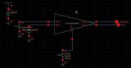
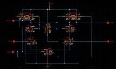
By the way, one of the sub-systems i am working on is the comparator. The comparator, as taken granted to be a block for most people that compares the 2 input and gives an indication of which is bigger at the output, requires some knowledge of the workings of the MOS transistor as an amplifier. I am actually quite impressed when i read and learn about how people implement the comparator, by making use of the characteristics of the op amp.
This is what goes on inside the black box, with current consumption of only 100nA!
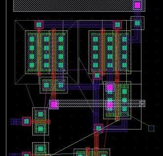
And layout is more messy, here is just a testing layout for me to practice on cos i haven't take EE4415 which deals with abit on layout design, which proves to be really useful as my teammates all like very pro in layout except me.. =((
Just attended the first lesson of this semester, which is EE4410 where the prof gave us a brief intro to the project that we are going to embark on. ECG signal acquisition system, which is to be designed and fabricated on a chip. Each project group consists of 4 people and each one is to design a subsystem of the chip, very much like EE2001, and then later integrate them together.
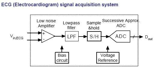
My part is going to be the ADC, which is quite challenging I would say. The architecture of this ADC is to be using the successive approximation algorithm, while my FYP is on another kind of architecture called the sigma delta modulation, which makes use of oversampling and noise shaping technique. From what I see now, both designs are quite hard one. Moreover, the dateline for the submission of the EE4410 final design is in week 9. This means the schematic design as well as the layout design to be ready for tape out. So, we have only around 2 months to complete this, which is really really rushed. I am so going to relive the days of EE2001 and eat, work, sleep on EE4410 everyday. Wait, there’s also my FYP hor? Wah, means eat, work, sleep on EE4410 and EE4001, like doing 2 FYPs.. Great, just great…
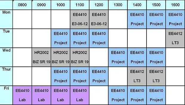
Now, some people went a bit crazy over the fact that my timetable in my previous entry was like so empty. Well, now to loosen them up a bit, here I posted another timetable which will very likely quite accurately reflects what I will be working on for the next month or so. It seems preposterous somewhat, but that’s really what my group intended to do. Complete the design by mid term and start worrying about our FYP.
Wish my good luck, will ya?